Wafer Defect Classifier
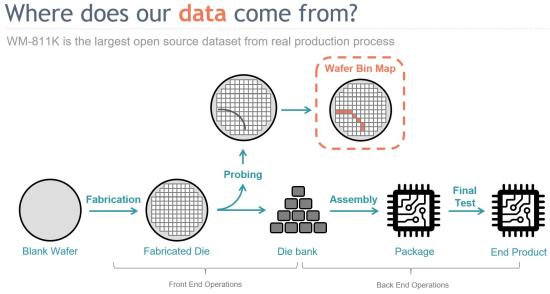
Semiconductor chips are used in a variety of applications (mobile phones, data centers, smart homes, security, to name a few) that drive integration of our life into the digital world. It is critical to achieve desired performance levels, high yield, and low cost of such chips to drive broad adoption in the industry. The manufacturing of these chips happens on 300mm silicon wafer, and the process is complex with hundreds of steps, equipment, and human interaction. During the manufacturing process, physical defects (particles, scratches) and variability (thickness, uniformity) can significantly affect yield and need to be controlled and eliminated. However, many times such defects might not be visible or detected at the point of occurrence and are only caught with electrical signals at end of line. This can be late in the process but still need to be correlated back to the source of defects so that the source can be fixed to avoid continued occurrence of such defects.
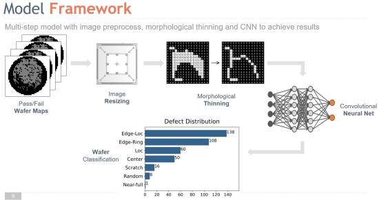
Our goal was to implement a model pipeline that uses a wafer image preprocessing and a neural network to help semiconductor manufacturers use pattern recognition to accurately detect the defect types and get to the root cause faster. Our final product takes wafer maps with electrical defect signatures as inputs and performs the following tasks.
- Classify wafers into good (no defect pattern) versus bad (with defect pattern)
- Identify defect pattern for the wafer (e.g., edge, center, donut, local, etc.)
- Identify if the defect pattern has happened before and the source of the defects


